- Home
- Products
- Automotive Connector
- Automotive Diagnostic Cable
- other
- plastic parts
- Dechi diagnose Cable
- Electronic products
- New energy charging CABLE
- OBD GPS Tracking Cables
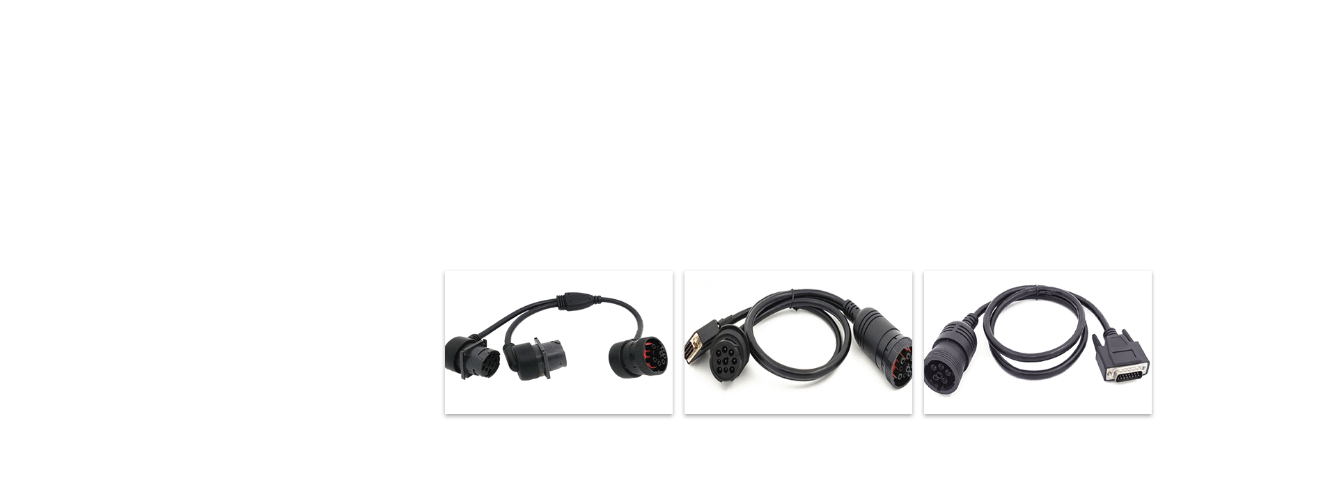
- OBD II Vehicle Diagnostic Cables
- OBD2 Splitter Y Cables
- OBDII Detection Cable
- OBDII Extension Cable
- PCBA
- Plastic molding class
- SMT
- Urea Pump Detection Line
- Waterproof Cable
- About Us
- Quality
- News
- Contact Us
- Product Name
- Product Keyword
- Product Model
- Product Summary
- Product Description
- Multi Field Search


")